
Scanning Electron Microscopy (SEM Analysis) Laboratory
Scanning Electron Microscopy (SEM Analysis) can produce images of almost any sample at magnifications of 15-300,000X. The SEM has tremendous depth of field allowing for imaging that cannot be accomplished using optical microscopy. Conductive and nonconductive samples can be imaged. When operated in the backscatter (BSE) detection mode, differences in material composition can be observed. Elemental analysis can be performed on any feature observed with an integrated Energy Dispersive Spectroscopy (EDS) detector.
SEM EDS analysis or SEM EDX analysis Laboratory can be used to provide chemical analysis in areas as small as one micrometer in diameter.


Scanning Electron Microscopy (SEM)
In the SEM, an electron beam is focused into a fine probe and rastered over a small rectangular area. As the electrons interact with the sample, various signals, including those from secondary electrons, are created and detected. These highly localized signals are used to modulate the brightness of a CRT display rastered synchronously with the electron beam. The image formed on the CRT is a highly magnified image of the sample. The technique is usually nondestructive, although instrumental sample requirements often mandate alteration of the sample before analysis. Magnification is from 10X to 300,000X and lateral resolution is 10-50nm, allowing features as small as 100 Å to be seen. The analysis depth is 20-50 Å. SEM Analysis provides excellent topographical data, and in backscatter mode atomic number information (compositional) also. Images can be e-mailed or delivered on various storage media for client manipulation.
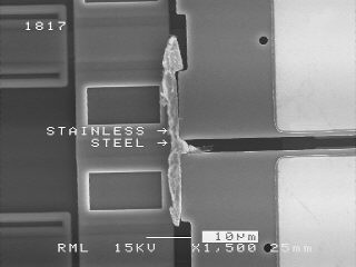
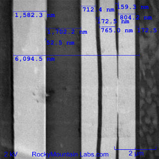
Back-Scattered Electron Images
Back-scattered electron (BSE) images are useful for locating phase differences and finding specific features on a sample. When a high energy electron interacts with an atom, it undergoes either inelastic scattering with the nucleus. BSEs result from elastic scattering and leave the sample with energies comparable to the primary beam. The likelihood of backscattering increases with the atomic number (Z) of the material. High-Z materials give a stronger signal (brightness) than low-Z materials, thereby giving image contrast from elemental differences.
What is Scanning Electron Microscopy (SEM Analysis)?
Scanning Electron Microscopy (SEM) is a powerful imaging technique used to study the surface morphology and composition of a wide variety of samples at high magnifications. In SEM analysis, a beam of high-energy electrons is focused on the sample surface, which causes the emission of secondary electrons, backscattered electrons, and other signals. These signals are detected and analyzed to produce high-resolution images of the sample surface, providing information on its topography, texture, and elemental composition.
SEM is particularly useful for studying materials with complex surface structures or features that cannot be seen with other types of microscopes, such as optical microscopes. In addition to imaging, SEM can also be used for other types of analysis, such as elemental analysis (EDX) and surface charge (ESCA).
SEM analysis provides researchers with a powerful tool for studying the microscopic world, enabling them to gain a deeper understanding of the structure, properties, and behavior of a wide variety of materials.
How does Scanning Electron Microscopy (SEM Analysis) work?
Scanning Electron Microscopy Laboratory (SEM) works by directing a beam of high-energy electrons onto the sample surface and detecting the various signals that are produced as a result. The basic steps involved in SEM analysis are as follows:
- Sample preparation: The sample must first be prepared for analysis, which typically involves cleaning and drying it to remove any surface contaminants or moisture that could interfere with the imaging process.
- Imaging: The sample is then placed in the SEM chamber, and a high-energy electron beam is generated and focused onto the sample surface using a series of electromagnetic lenses. As the beam interacts with the sample, it generates various signals, including secondary electrons and backscattered electrons.
- Signal detection: The various signals generated by the beam-sample interaction are detected by specialized detectors located within the SEM chamber. Secondary electrons, for example, are typically detected by a secondary electron detector (EDS), while backscattered electrons are detected by a backscattered electron detector (BSD).
- Image formation: The signals detected by the SEM are then processed and used to generate an image of the sample surface. The resulting images can be highly detailed, with resolutions ranging from a few nanometers to tens of nanometers, depending on the imaging conditions and the sample properties.
- Analysis: The images generated by the SEM can be used for a wide range of qualitative and quantitative analyses, including morphological characterization, elemental composition, crystallography, and surface charge.
SEM analysis works by directing a beam of high-energy electrons onto the sample surface and detecting the various signals generated by the beam-sample interaction to produce high-resolution images and other types of analysis.
Scanning Electron Microscopy (SEM Analysis) Process
The process of Scanning Electron Microscopy (SEM) analysis involves several steps, including sample preparation, imaging, signal detection, image formation, and analysis. Here is a more detailed description of each step:
- Sample Preparation: This step involves preparing the sample for SEM analysis. The sample is typically cleaned and dried to remove any surface contaminants or moisture that could interfere with the imaging process. It is then coated with a thin layer of conducting material, such as gold or carbon, to improve its conductivity and reduce charging effects during imaging.
- Imaging: Once the sample is prepared, it is placed in the SEM chamber, and a beam of high-energy electrons is generated and focused onto the sample surface using a series of electromagnetic lenses. As the beam interacts with the sample, it generates various signals, including secondary electrons, backscattered electrons, and X-rays.
- Signal Detection: The various signals generated by the beam-sample interaction are detected by specialized detectors located within the SEM chamber. Secondary electrons, for example, are typically detected by a secondary electron detector (SED), while backscattered electrons are detected by a backscattered electron detector (BSD).
- Image Formation: The signals detected by the SEM are then processed and used to generate an image of the sample surface. The resulting images can be highly detailed, with resolutions ranging from a few nanometers to tens of nanometers, depending on the imaging conditions and the sample properties.
- Analysis: Once the image is formed, it can be used for a wide range of qualitative and quantitative analyses, including morphological characterization, elemental composition, crystallography, and surface charge. The analysis can involve manual interpretation of the image or automated image analysis using specialized software.
SEM analysis is a powerful imaging technique that provides researchers with a wealth of information about the surface morphology, composition, and structure of a wide variety of materials and biological systems.
Principles of Scanning Electron Microscopy (SEM Analysis)
Scanning Electron Microscopy (SEM) is based on several principles that allow the imaging of the surface of a sample at high magnification and resolution. The main principles of SEM analysis are:
- Electron beam generation: The SEM generates a beam of high-energy electrons using an electron gun, which is typically made up of a filament and an electrode. The filament is heated to emit electrons, which are then focused by the electrode into a fine beam.
- Electron-sample interaction: The focused electron beam is then directed onto the sample surface, and as the beam interacts with the sample, it generates various signals, including secondary electrons and backscattered electrons. These signals provide information about the surface topography, composition, and crystal structure of the sample.
- Signal detection: The various signals generated by the beam-sample interaction are detected by specialized detectors located within the SEM chamber. Secondary electrons, for example, are typically detected by a secondary electron detector (EDS), while backscattered electrons are detected by a backscattered electron detector (BSD).
- Image formation: The signals detected by the SEM are then processed and used to generate an image of the sample surface. The image formation can be done in two ways: either by scanning the electron beam across the sample surface and measuring the intensity of the various signals at each point, or by detecting the signals emitted from the sample while the sample is being rotated.
- Analysis: Once the image is formed, it can be used for a wide range of qualitative and quantitative analyses, including morphological characterization, elemental composition and surface charge.
SEM analysis is based on the principles of electron beam generation, electron-sample interaction, signal detection, image formation, and analysis. These principles allow researchers to study the surface morphology and composition of a wide variety of samples at high magnifications and resolutions, making SEM a powerful tool in materials science and other fields.
Applications of Scanning Electron Microscopy (SEM Analysis)
Scanning Electron Microscopy (SEM) analysis has a wide range of applications in various fields. Some of the major applications of SEM analysis are:
- Material characterization: SEM analysis can be used to study the surface morphology and composition of a wide range of materials, including metals, ceramics, polymers, and composites. It can also be used to investigate the microstructure of materials and to identify defects and failure mechanisms.
- Nanotechnology: SEM analysis is an essential tool in the field of nanotechnology, where it is used to study the morphology, composition, and structure of nanoparticles and nanomaterials. SEM can also be used to measure the size, shape, and distribution of nanoparticles.
- Semiconductor industry: SEM analysis is an essential tool in the semiconductor industry, where it is used to study the morphology and composition of semiconductor materials and devices.
SEM analysis is a versatile and powerful tool that has a wide range of applications in various fields, providing researchers with valuable insights into the morphology, composition, and structure of materials.
Where is Scanning Electron Microscopy (SEM Analysis) used?
Scanning Electron Microscopy (SEM) analysis is used in a wide range of industries and fields, including:
- Materials Science: SEM is used to study the microstructure, morphology, and composition of materials such as metals, ceramics, polymers, and composites. It is also used to investigate the surface properties of materials, such as adhesion, friction, and wear.
- Semiconductor Industry: SEM is used to study the microstructure and composition of semiconductor materials and devices, such as transistors, diodes, and integrated circuits. It is also used to investigate the failure mechanisms of these devices.
- Nanotechnology: SEM is used to study the morphology and composition of nanomaterials and nanoparticles. It is also used to investigate the properties and behavior of these materials at the nanoscale.
SEM analysis is used in a wide range of industries and fields, providing valuable insights into the morphology, composition, and structure of materials and biological systems.
Industries which need Scanning Electron Microscopy (SEM Analysis)
Scanning Electron Microscopy (SEM) analysis is used in many industries that rely on advanced materials or require a detailed understanding of surface morphology and composition. Some of the industries that frequently use SEM analysis include:
- Materials Science: The materials science industry uses SEM analysis to study the microstructure and composition of advanced materials such as alloys, polymers, and composites. This information is essential for developing new materials with improved properties and understanding how materials will perform in different applications.
- Semiconductor Industry: The semiconductor industry relies heavily on SEM analysis to investigate the microstructure and composition of semiconductor devices such as transistors, diodes, and integrated circuits. This information is critical for optimizing device performance and improving device reliability.
- Medical Device Industry: The medical device industry uses SEM analysis to study the surface properties and morphology of medical devices, including implants, prosthetics, and surgical instruments. This information is essential for optimizing device performance and ensuring that devices are safe for use in patients.
- Nanotechnology: The nanotechnology industry relies heavily on SEM analysis to study the morphology and composition of nanoparticles and nanomaterials. This information is critical for developing new nanomaterials with unique properties and understanding how these materials will behave in different environments.
- Aerospace Industry: The aerospace industry uses SEM analysis to study the microstructure and composition of advanced materials used in aircraft, spacecraft, and other aerospace applications. This information is essential for ensuring that these materials can withstand the extreme conditions of aerospace environments.
- Automotive Industry: The automotive industry uses SEM analysis to study the microstructure and composition of advanced materials used in engines, transmissions, and other automotive components. This information is critical for optimizing component performance and improving vehicle efficiency.
SEM analysis is a valuable tool in many industries, providing essential insights into the morphology, composition and structure of materials.
Strengths and Limitations Scanning Electron Microscopy (SEM Analysis)
Scanning Electron Microscopy (SEM) analysis has many strengths and limitations, which should be considered when deciding whether to use this technique for a particular application. Some of the key strengths and limitations of SEM analysis include:
Strengths:
- High Resolution: SEM analysis can provide high-resolution images of the surface morphology of samples, with sub-nanometer resolution possible in some cases. This makes it an ideal technique for investigating the surface features and topography of materials.
- Large Depth of Field: SEM analysis has a large depth of field, which means that a wide range of sample depths can be imaged in a single image. This makes it possible to capture detailed images of complex samples with varying topographies.
- Composition Information: SEM analysis can provide information on the composition of samples through the use of energy-dispersive X-ray spectroscopy (EDS). This allows researchers to identify the elemental composition of materials.
- Non-destructive: SEM analysis is a non-destructive technique, which means that samples can be imaged without damaging them. This is important when investigating delicate or valuable samples.
Limitations:
- Sample Preparation: SEM analysis requires extensive sample preparation. This can be time-consuming and may alter the sample’s structure or properties.
- Vacuum Conditions: SEM analysis requires samples to be imaged under high vacuum conditions, which may not be suitable for some samples, such as those containing volatile or reactive compounds.
- Sample Size Limitations: SEM analysis is typically limited to small sample sizes due to the need for high vacuum conditions and the use of small sample holders.
- Cost: SEM analysis equipment can be expensive to purchase and maintain, which may limit access to this technique for some researchers and organizations.
SEM analysis is a powerful technique for investigating the surface morphology and composition of materials but its strengths and limitations should be considered when deciding whether to use this technique for a particular application.